Electron-Beam Assisted Nanoprocess
System
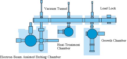
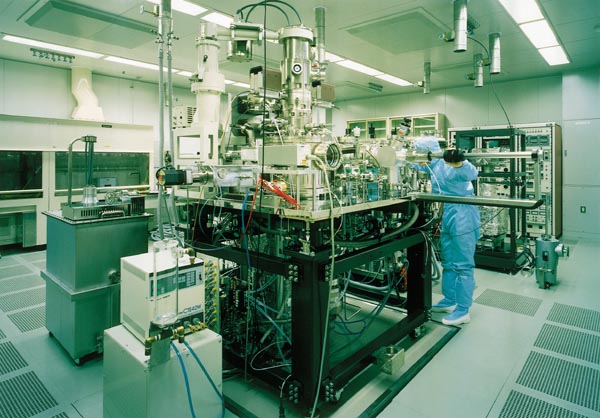 This
equipment is one of the main systems in this laboratory that we
believe to be essential for the realization of next-generation,
highly functional, nanoscale electron devices. Its key components
consist of an electron-beam-assisted (EB-assisted) etching and
a molecular beam epitaxy (MBE) system. These two subsystems are
connected to each other by an ultra-high vacuum transfer chamber.
This
equipment is one of the main systems in this laboratory that we
believe to be essential for the realization of next-generation,
highly functional, nanoscale electron devices. Its key components
consist of an electron-beam-assisted (EB-assisted) etching and
a molecular beam epitaxy (MBE) system. These two subsystems are
connected to each other by an ultra-high vacuum transfer chamber.
The EB-assisted etching system is composed of a high-energy
(100 keV) small diameter (< 3 nm) electron beam gun, a reactive
etching gas introduction device, and an UHV etching chamber (<
5x10⁻¹⁰ Torr).
The MBE system consists of an UHV (< 5x10-11 Torr) thin
film (< 1 nm) growth chamber, a baking chamber, and a loading
chamber.
This system allows us to alternate nano-scale pattern writing
and thin film growth without contaminating the surface of the
wafer by exposure to air.
Research Topics
üť In situ ultrahigh-vacuum process technology
üťEB-assisted untrafine-pattern lithography
üťFabrication of quantum nanostructures such as quantum dots and
quantum wires
üťTransport and optical properties of quantum nanostructures
üťApplication of quantum nanostructures to new devices
üťAtomically controlled super-heteroepitaxy